- 您现在的位置:买卖IC网 > Sheet目录2006 > LTC2754AIUKG-16#PBF (Linear Technology)IC DAC 16BIT QUAD IOUT 52-QFN
LTC2754
12
2754f
TIMING DIAGRAMS
Output Ranges
The LTC2754 is a quad, current-output, serial-input preci-
sion multiplying DAC with selectable output ranges. Ranges
can either be programmed in software for maximum
exibility—each of the four DACs can be programmed
to any one of six output ranges—or hardwired through
pin-strapping. Two unipolar ranges are available (0V to 5V
and 0V to 10V), and four bipolar ranges (±2.5V, ±5V, ±10V
and –2.5V to 7.5V). These ranges are obtained when an
external precision 5V reference is used. When a reference
voltage of 2V is used, the ranges become: 0V to 2V, 0V to
4V, ±1V, ±2V, ±4V and –1V to 3V. The output ranges are
linearly scaled for other reference voltages.
Manual Span Conguration
Multiple output ranges are not needed in some applica-
tions. To congure the LTC2754 to operate in a single span
without additional operational overhead, tie the M-SPAN
pin directly to VDD. The active output range for all four
DACs is then set via hardware pin strapping of pins S2,
S1 and S0 (rather than through the SPI port); and Write
and Update commands have no effect on the active output
span. See Figure 1 and Table 3.
Tie the M-SPAN pin to ground for normal SoftSpan
operation.
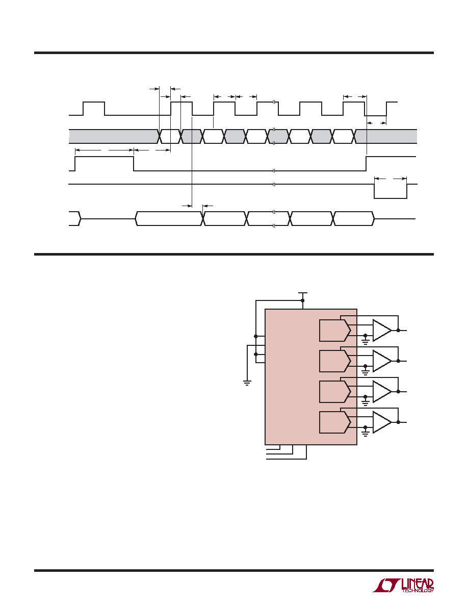
Figure 1. Using M-SPAN to Congure the LTC2754
for Single-Span Operation (±10V Range Shown).
LTC2754-16
M-SPAN
S2
S1
S0
2754 F01
CS/LD SDI SCK
VDD
DAC A
±10V
DAC B
DAC C
DAC D
–
+
–
+
–
+
–
+
SDI
SRO
Hi-Z
CS/LD
SCK
LSB
2754 TD
LSB
t2
t9
t8
t5
t7
1
2
31
32
t6
t1
LDAC
t3
t4
t11
OPERATION
发布紧急采购,3分钟左右您将得到回复。
相关PDF资料
LTC2755AIUP-16#PBF
IC DAC 16BIT CUR OUT 64-QFN
LTC2757ACLX#PBF
IC DAC 18BIT PAR 48LQFP
LTC2758AILX#PBF
IC DAC 18BIT SPI/SRL 48-LQFP
LTC2844IG#TRPBF
IC TXRX 3.3V MULTIPROTCOL 28SSOP
LTC2852MPS#PBF
IC TXRX RS485 20MBPS 14-SOIC
LTC486ISW#TRPBF
IC DVR RS485 LOW PWR QUAD 16SOIC
LTC490IS8#TRPBF
IC TXRX RS485 LOW POWER 8-SOIC
LTC491IS#TRPBF
IC TXRX RS485 LOW POWER 14-SOIC
相关代理商/技术参数
LTC2754AIUKG-16#TRPBF
功能描述:IC DAC 16BIT QUAD IOUT 52-QFN RoHS:是 类别:集成电路 (IC) >> 数据采集 - 数模转换器 系列:SoftSpan™ 产品培训模块:Data Converter Fundamentals
DAC Architectures 标准包装:750 系列:- 设置时间:7µs 位数:16 数据接口:并联 转换器数目:1 电压电源:双 ± 功率耗散(最大):100mW 工作温度:0°C ~ 70°C 安装类型:表面贴装 封装/外壳:28-LCC(J 形引线) 供应商设备封装:28-PLCC(11.51x11.51) 包装:带卷 (TR) 输出数目和类型:1 电压,单极;1 电压,双极 采样率(每秒):143k
LTC2754BCUKG-16#PBF
功能描述:IC DAC 16BIT QUAD IOUT 52-QFN RoHS:是 类别:集成电路 (IC) >> 数据采集 - 数模转换器 系列:SoftSpan™ 标准包装:1 系列:- 设置时间:4.5µs 位数:12 数据接口:串行,SPI? 转换器数目:1 电压电源:单电源 功率耗散(最大):- 工作温度:-40°C ~ 125°C 安装类型:表面贴装 封装/外壳:8-SOIC(0.154",3.90mm 宽) 供应商设备封装:8-SOICN 包装:剪切带 (CT) 输出数目和类型:1 电压,单极;1 电压,双极 采样率(每秒):* 其它名称:MCP4921T-E/SNCTMCP4921T-E/SNRCTMCP4921T-E/SNRCT-ND
LTC2754BCUKG-16#TRPBF
功能描述:IC DAC 16BIT QUAD IOUT 52-QFN RoHS:是 类别:集成电路 (IC) >> 数据采集 - 数模转换器 系列:SoftSpan™ 产品培训模块:Data Converter Fundamentals
DAC Architectures 标准包装:750 系列:- 设置时间:7µs 位数:16 数据接口:并联 转换器数目:1 电压电源:双 ± 功率耗散(最大):100mW 工作温度:0°C ~ 70°C 安装类型:表面贴装 封装/外壳:28-LCC(J 形引线) 供应商设备封装:28-PLCC(11.51x11.51) 包装:带卷 (TR) 输出数目和类型:1 电压,单极;1 电压,双极 采样率(每秒):143k
LTC2754BIUKG-16#PBF
功能描述:IC DAC 16BIT QUAD IOUT 52-QFN RoHS:是 类别:集成电路 (IC) >> 数据采集 - 数模转换器 系列:SoftSpan™ 产品培训模块:Data Converter Fundamentals
DAC Architectures 标准包装:750 系列:- 设置时间:7µs 位数:16 数据接口:并联 转换器数目:1 电压电源:双 ± 功率耗散(最大):100mW 工作温度:0°C ~ 70°C 安装类型:表面贴装 封装/外壳:28-LCC(J 形引线) 供应商设备封装:28-PLCC(11.51x11.51) 包装:带卷 (TR) 输出数目和类型:1 电压,单极;1 电压,双极 采样率(每秒):143k
LTC2754BIUKG-16#TRPBF
功能描述:IC DAC 16BIT QUAD IOUT 52-QFN RoHS:是 类别:集成电路 (IC) >> 数据采集 - 数模转换器 系列:SoftSpan™ 产品培训模块:Data Converter Fundamentals
DAC Architectures 标准包装:750 系列:- 设置时间:7µs 位数:16 数据接口:并联 转换器数目:1 电压电源:双 ± 功率耗散(最大):100mW 工作温度:0°C ~ 70°C 安装类型:表面贴装 封装/外壳:28-LCC(J 形引线) 供应商设备封装:28-PLCC(11.51x11.51) 包装:带卷 (TR) 输出数目和类型:1 电压,单极;1 电压,双极 采样率(每秒):143k
LTC2754CUKG-12#PBF
功能描述:IC DAC 12BIT QUAD IOUT 52-QFN RoHS:是 类别:集成电路 (IC) >> 数据采集 - 数模转换器 系列:SoftSpan™ 产品培训模块:Data Converter Fundamentals
DAC Architectures 标准包装:750 系列:- 设置时间:7µs 位数:16 数据接口:并联 转换器数目:1 电压电源:双 ± 功率耗散(最大):100mW 工作温度:0°C ~ 70°C 安装类型:表面贴装 封装/外壳:28-LCC(J 形引线) 供应商设备封装:28-PLCC(11.51x11.51) 包装:带卷 (TR) 输出数目和类型:1 电压,单极;1 电压,双极 采样率(每秒):143k
LTC2754CUKG-12#TRPBF
功能描述:IC DAC 12BIT QUAD IOUT 52-QFN RoHS:是 类别:集成电路 (IC) >> 数据采集 - 数模转换器 系列:SoftSpan™ 标准包装:47 系列:- 设置时间:2µs 位数:14 数据接口:并联 转换器数目:1 电压电源:单电源 功率耗散(最大):55µW 工作温度:-40°C ~ 85°C 安装类型:表面贴装 封装/外壳:28-SSOP(0.209",5.30mm 宽) 供应商设备封装:28-SSOP 包装:管件 输出数目和类型:1 电流,单极;1 电流,双极 采样率(每秒):*
LTC2754IUKG-12#PBF
功能描述:IC DAC 12BIT QUAD IOUT 52-QFN RoHS:是 类别:集成电路 (IC) >> 数据采集 - 数模转换器 系列:SoftSpan™ 产品培训模块:Data Converter Fundamentals
DAC Architectures 标准包装:750 系列:- 设置时间:7µs 位数:16 数据接口:并联 转换器数目:1 电压电源:双 ± 功率耗散(最大):100mW 工作温度:0°C ~ 70°C 安装类型:表面贴装 封装/外壳:28-LCC(J 形引线) 供应商设备封装:28-PLCC(11.51x11.51) 包装:带卷 (TR) 输出数目和类型:1 电压,单极;1 电压,双极 采样率(每秒):143k